


Printed Circuit Board Factory: The Silent Cornerstone of Modern Electronics
Printed Circuit Board Factory: The Silent Cornerstone of Modern Electronics
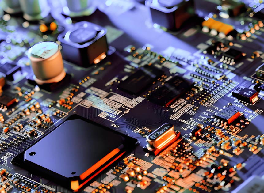
At the heart of every smartphone, computer, automobile, and smart appliance we use daily lies a critical component—the Printed Circuit Board (PCB). The place where these complex "nervous systems" are manufactured is the Printed Circuit Board Factory. It is far more than a simple assembly workshop; it is an advanced manufacturing center that integrates precision machinery, chemistry, materials science, and computer technology, rightfully serving as the silent cornerstone of the modern electronics industry.
Part 1: Core Product: What is a PCB?
A Printed Circuit Board is a fundamental component used to mount electronic components and facilitate electrical connections between them through copper traces on its surface and inner layers. It provides structural support, ensuring the orderly and efficient flow of electronic signals and power.
Part 2: The Core Manufacturing Process in a PCB Factory
PCB manufacturing is an extremely complex, multi-step precision process. The key stages can be summarized as follows:
1. Design and Photoplotting
-
Everything begins with the engineer‘s electronic design. The design files are sent to the factory and used to produce "films" for the subsequent exposure process—the phototools. These are the blueprints for the PCB.
2. Inner Layer Fabrication (for Multi-layer Boards)
-
Panel Sizing: Large sheets of copper-clad laminate (insulating substrate covered with copper foil) are cut into production panels.
-
Inner Layer Imaging: The circuit pattern is transferred onto the copper foil by coating with photoresist, exposure (using phototools), and development.
-
Etching: Chemicals etch away the unwanted copper from non-circuit areas, leaving behind the required precision circuits.
-
Automated Optical Inspection (AOI): High-precision scanners inspect the inner layer circuits for defects.
3. Lamination
-
The prepared inner layer cores, prepreg (pre-impregnated material), and outer layer copper foil are precisely stacked like a layered structure and bonded into a solid multi-layer board under high temperature and pressure.
4. Drilling
-
Extremely fine drill bits or lasers are used to drill through-holes, blind vias, and buried vias in the board to interconnect different layer circuits. This is a high-precision step critical for electrical connectivity.
5. Plating & Outer Layer Imaging
-
Electroless Copper Deposition: A thin layer of chemical copper is deposited on the non-conductive hole walls to make them conductive.
-
Electroplating: Electroplating thickens the copper on the hole walls and board surface, ensuring connection reliability.
-
Subsequently, a process similar to outer layer imaging is carried out to form the outer layer circuits.
6. Solder Mask & Surface Finish
-
Solder Mask: A layer of green (or other colors) solder mask ink is applied to cover non-soldering areas, preventing solder shorts and providing insulation.
-
Surface Finish: The exposed pads undergo treatment—such as HASL, ENIG, Immersion Silver, or OSP—to ensure good solderability and long-term reliability.
7. Silkscreen & Fabrication/Final Testing
-
Silkscreen: Component designators, logos, and other markings are printed onto the board.
-
Panel Depaneling: The large production panel is routed or scored (V-CUT) into individual small boards.
-
Electrical Test: A final continuity test (e.g., Flying Probe or Fixture Test) is performed to ensure each PCB is free from open or short circuits.
Part 3: The Importance and Challenges of a PCB Factory
Importance:
-
Foundation of the Electronics Industry: Virtually no modern electronic product could exist without PCBs.
-
Vehicle for Technological Innovation: Advancements in electronic technologies—from 5G and AI to IoT—are directly reflected in increasing demands on PCBs, such as higher frequencies, smaller sizes, and more layers.
Challenges:
-
High Technical Complexity: Involves multiple disciplines and requires extremely strict control of process parameters.
-
Significant Environmental Pressure: The chemicals and heavy metals (like copper) used in production necessitate complex wastewater and exhaust treatment systems to meet emission standards and enable recycling.
-
Capital Intensity: High-end equipment (e.g., laser drills, direct imaging systems, AOI) is expensive, leading to very high factory setup and maintenance costs.
-
Intense Market Competition: Products require a delicate balance between high quality, low cost, and fast delivery.
Part 4: Future Trends
The future PCB factory is moving towards "Smart Manufacturing" and "Green Practices."
-
Industry 4.0: Leveraging IoT, Big Data, and AI for real-time production monitoring, predictive maintenance, and quality optimization, paving the way for "lights-out" factories.
-
Advanced Materials & Processes: Developing substrate materials for high-frequency/high-speed applications and finer line processing technologies.
-
Sustainable Development: Promoting energy conservation, emission reduction, and the use of more environmentally friendly raw materials and processes to reduce the carbon footprint.
Conclusion
A Printed Circuit Board factory is far from a traditional manufacturing site. It is a hall of precision artistry that constructs the connective skeleton of modern civilization on a microscopic scale. As we enjoy the conveniences brought by rapidly evolving electronic technology, we should not forget that it is these highly automated and technology-intensive factories that silently lay the digital foundation for it all.

 Mailme